The printed electronics industry has seen significant growth over the past decade, with advancements in materials, manufacturing techniques, and novel applications. One technology that has been instrumental in pushing the boundaries of printed electronics is ultraviolet (UV) curing systems. These systems use UV light to initiate a rapid, controlled polymerization process that solidifies inks and coatings on various substrates.
UV curing systems typically consist of three key components: a UV light source, a photosensitive material (such as ink or coating), and a substrate on which the material is applied. The UV light initiates a photopolymerization process that quickly transforms the liquid photosensitive material into a solid, stable form. This curing process provides several advantages over conventional drying methods, such as faster curing times, reduced energy consumption, and increased durability of the printed material.
Benefits of UV Curing Systems for Printed Electronics
Faster production speeds: The rapid curing time of UV-cured materials allows for high-speed printing processes, significantly reducing the time required for each production cycle. This translates to reduced downtime, higher output, and increased capacity to meet growing demand for printed electronics.
Enhanced durability: The UV curing process results in a strong bond between the photosensitive material and the substrate, leading to improved mechanical and chemical resistance. This ensures that printed electronic components can withstand harsh environments, such as extreme temperatures, humidity, and exposure to chemicals, making them suitable for a variety of applications.
Environmentally friendly: UV curing systems consume less energy compared to traditional thermal curing methods, reducing the overall carbon footprint of the manufacturing process. Additionally, since UV-cured materials generate fewer volatile organic compounds (VOCs) during the curing process, there is a significant reduction in air pollution and waste disposal concerns.
Increased design flexibility: UV curing systems enable the printing of intricate patterns and structures on various substrates, allowing for greater design freedom. This facilitates the development of innovative printed electronics solutions, such as conformable sensors, flexible displays, and miniaturized components for various applications.
Applications of UV Curing Systems in Printed Electronics
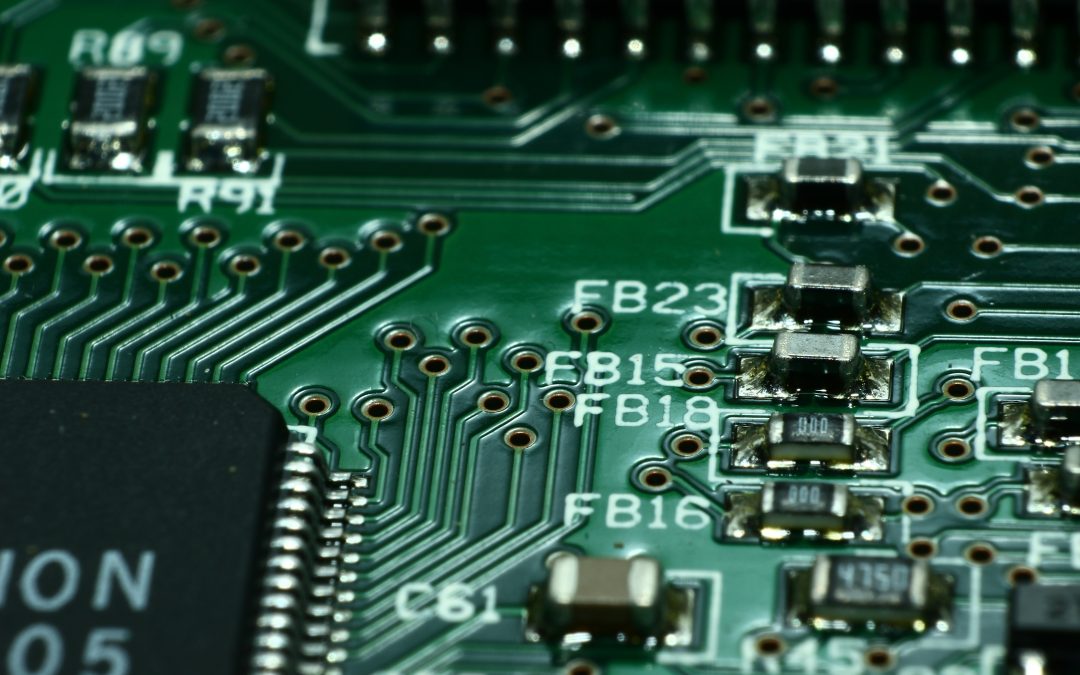
Printed circuit boards (PCBs): The use of UV curing systems in the PCB manufacturing process has led to significant improvements in resolution and layer alignment. This enables the production of high-density, multi-layer PCBs with smaller feature sizes, which are essential for compact electronic devices.
Flexible electronics: The rapid curing process makes it possible to print electronic components on flexible substrates, such as polyimide films or textile materials. This has opened up new possibilities for wearable devices, medical sensors, and other applications where flexibility and conformability are required.
OLED displays: UV-cured materials can be used to create stable and efficient organic layers for OLED displays, resulting in higher brightness, longer lifetimes, and improved power efficiency. This technology is increasingly being adopted in smartphones, televisions, and other consumer electronics products.
Printed sensors: UV curing systems have facilitated the production of robust, high-performance printed sensors for various applications. Examples include pressure sensors for automotive safety systems, gas sensors for environmental monitoring, and biosensors for medical diagnostics. The versatility of UV-cured materials allows for the development of innovative sensor designs with improved sensitivity and durability.
UV curing systems have already made a significant impact on the printed electronics industry, and their influence will only grow as the technology continues to evolve. The ongoing development and adoption of UV curing systems will facilitate the creation of more efficient, sustainable, and versatile electronic devices and applications, ultimately shaping the future of printed electronics and driving innovation across various industries.
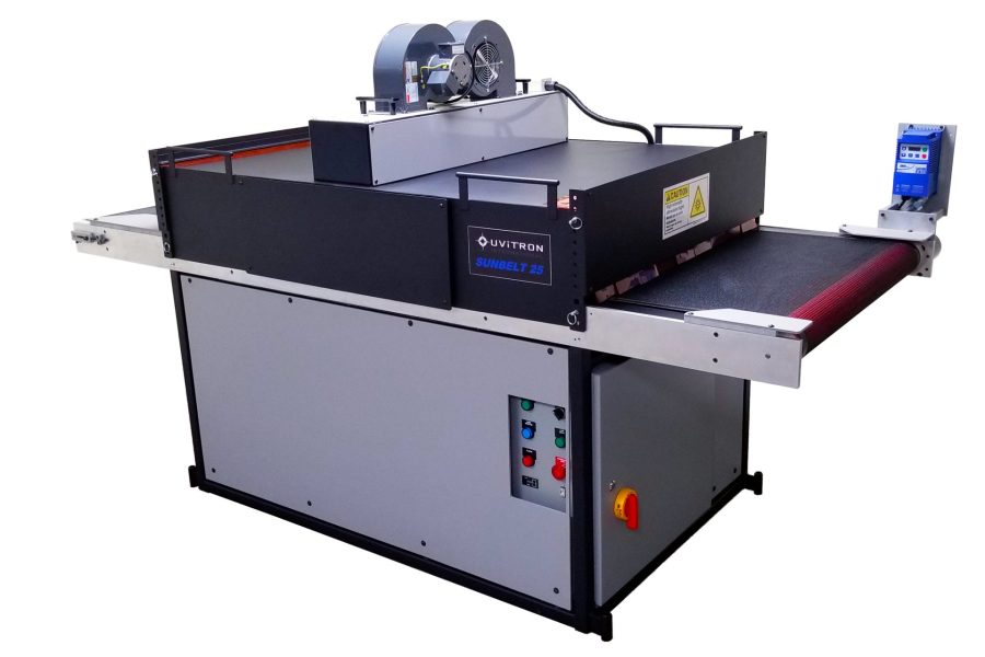
Sunbelt 25 UV Conveyor
The Uvitron SunBelt 25, with its wide-width and high-power light-curing capabilities, is perfectly suited to meet the increasing demands of the printed electronics industry. Its unique features make it an ideal solution for various applications in this sector, providing efficient and reliable UV curing for high volume production or large parts processing in laboratory settings.
Printed Circuit Boards (PCBs): The Uvitron SunBelt 25’s high-output arc lamp and programmable electronic power regulating ballast ensure precise, consistent curing of photosensitive materials used in PCB manufacturing. Its wide conveyor belt can accommodate large PCBs or multiple smaller boards, significantly increasing throughput and productivity. In addition, the SunBelt 25 can also be used to secure electronic components to PC board assemblies using UV adhesives, and to seal portions of the assemblies using UV cured form-in-place gaskets. The SunBelt 25 can also encapsulate small PC boards in UV cured potting compounds for shock and vibration protection or to prevent tampering or reverse engineering of sensitive board designs.
Flexible Electronics: The variable-speed motor and velocity regulating drive of the SunBelt 25 allow for precise control over curing times, ensuring that flexible substrates are not damaged or warped during the curing process. This is particularly important when manufacturing flexible electronic components such as wearable devices, sensors, or displays.
Large-Scale Printed Sensors: The SunBelt 25’s long, enclosed UV curing tunnel enables the efficient production of large-scale printed sensors or multiple smaller sensors simultaneously. Its entrance and exit light guards provide maximum light shielding, ensuring uniform curing and reducing the risk of overexposure or underexposure.
Displays and Lighting: The Uvitron SunBelt 25 can be utilized to cure organic layers in displays and lighting applications, providing a reliable and efficient solution for manufacturing these products. Its precise curing capabilities help to ensure optimal performance, stability, and longevity of the final product.
Research and Development: Laboratories working on the development of new materials, processes, or applications in printed electronics can benefit from the SunBelt 25’s precise curing control, wide conveyor belt, and high-output arc lamp. This system allows researchers to effectively test and optimize curing parameters for various materials and substrates, accelerating the development of innovative solutions in the printed electronics sector.
In conclusion, the Uvitron SunBelt 25 is a versatile UV curing system that can significantly enhance the manufacturing and development of printed electronics. Its unique features, such as the high-output arc lamp, wide conveyor belt, and precise curing control, make it a valuable tool for various applications within the industry, ultimately contributing to improved efficiency, productivity, and innovation.
CLICK HERE TO CUSTOMIZE YOUR SUNBELT 25 CONVEYOR SYSTEM